Nederlands
Transmission electron microscope
A transmission electron microscope fires electrons through an ultra-thin sample and so produces images in which you can even see rows of atoms. It is widely used for chips and materials.
A transmission electron microscope, abbreviated TEM, uses electrons instead of light to look at very small things. The electrons go straight through the sample ('transmission' means letting through), and an image forms behind the sample. A TEM can see details of about a tenth of a nanometre or smaller. That is fine enough for rows of atoms.
How does it work?
An ordinary microscope is limited by the wavelength of light: details smaller than that become blurred. Electrons also behave like waves, but with a much shorter wavelength, especially at a high voltage. That lets you see much finer details.
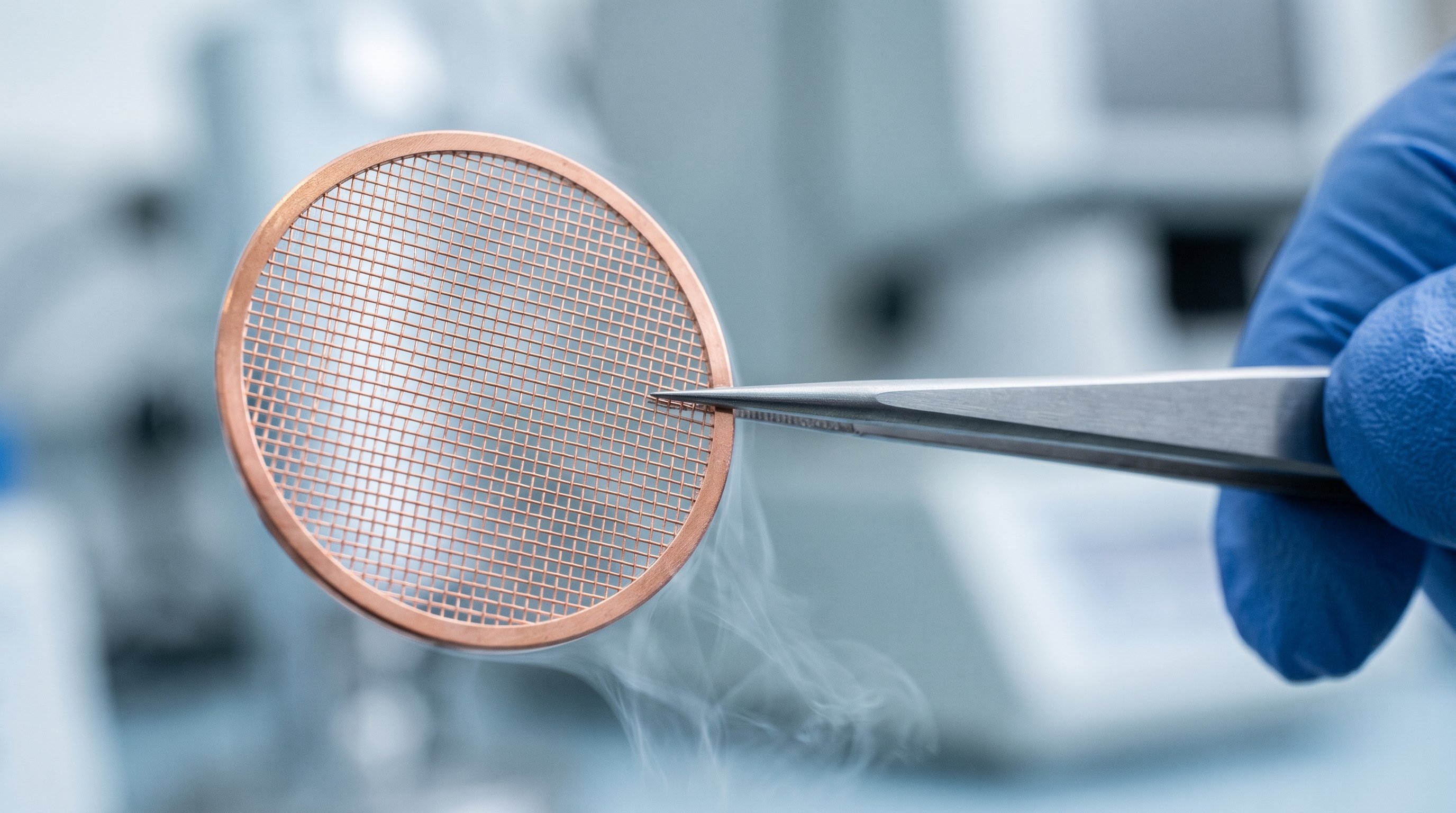
In a TEM, a high voltage accelerates the electrons into a narrow beam. Magnetic coils act as lenses and focus that beam on the sample. The sample has to be wafer-thin, often only a few tens of nanometres, otherwise the electrons cannot get through. Behind the sample, a detector converts the electrons into an image. Where the material is denser or has heavier atoms, more electrons are stopped and the image looks darker. The whole instrument works in a vacuum, because in air the electrons would collide with air molecules.
Why it matters
A lot of technology revolves around structures that are too small for ordinary microscopes, such as the layers and wiring in a chip, the materials in a battery or the make-up of a new material. With a TEM, researchers and manufacturers can see whether such a structure is right and why something does or does not work. That is useful for developing chips, batteries and other new materials, and also for checking what has really been made.
Articles about Transmission electron microscope
-
Anthropic uses AI to determine, for the first time, the shape of a puzzling protein shell from the bacterial world
Anthropic's biology team has used its AI assistant Claude to determine, for the first time, the 3D shape of a vault from the bacterial world: a hollow protein shell made with a protein from a bacterial virus. What such shells do in cells is now being studied further.