Nederlands
Cornell builds first working transistor from semiconductor with the widest band gap ever
Researchers at Cornell University made a semiconductor with a band gap of more than 7 electronvolts, the widest ever in a working device, and built a diode and a transistor from it. It is still lab work, but it could lead to more efficient electronics for high voltages.
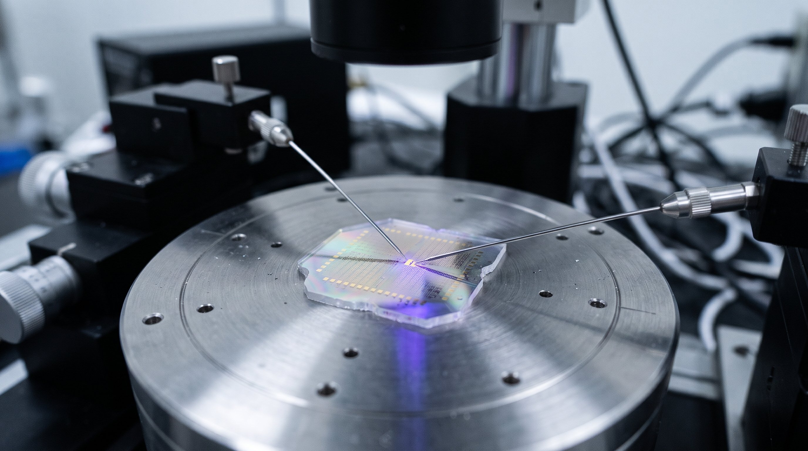
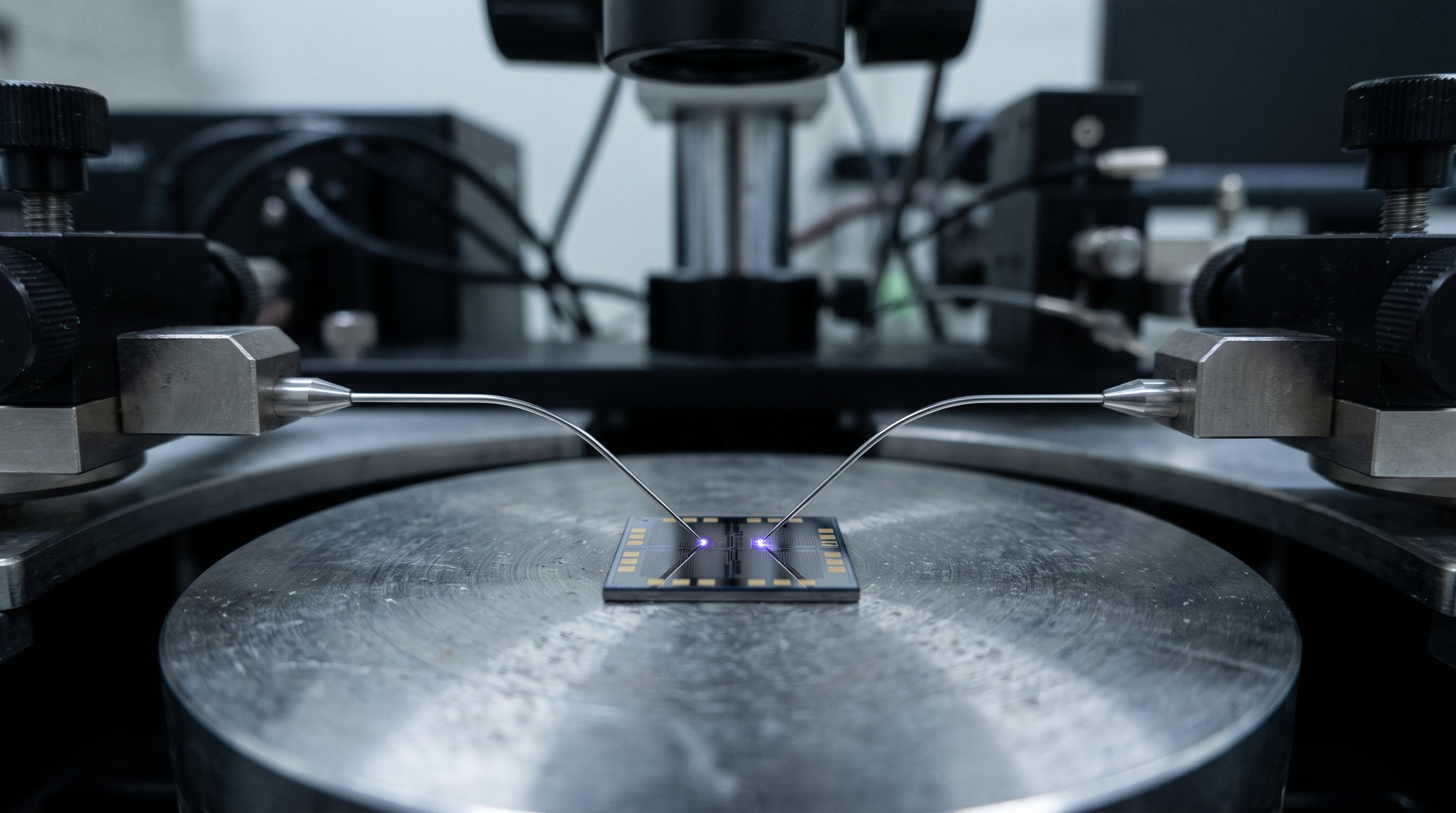
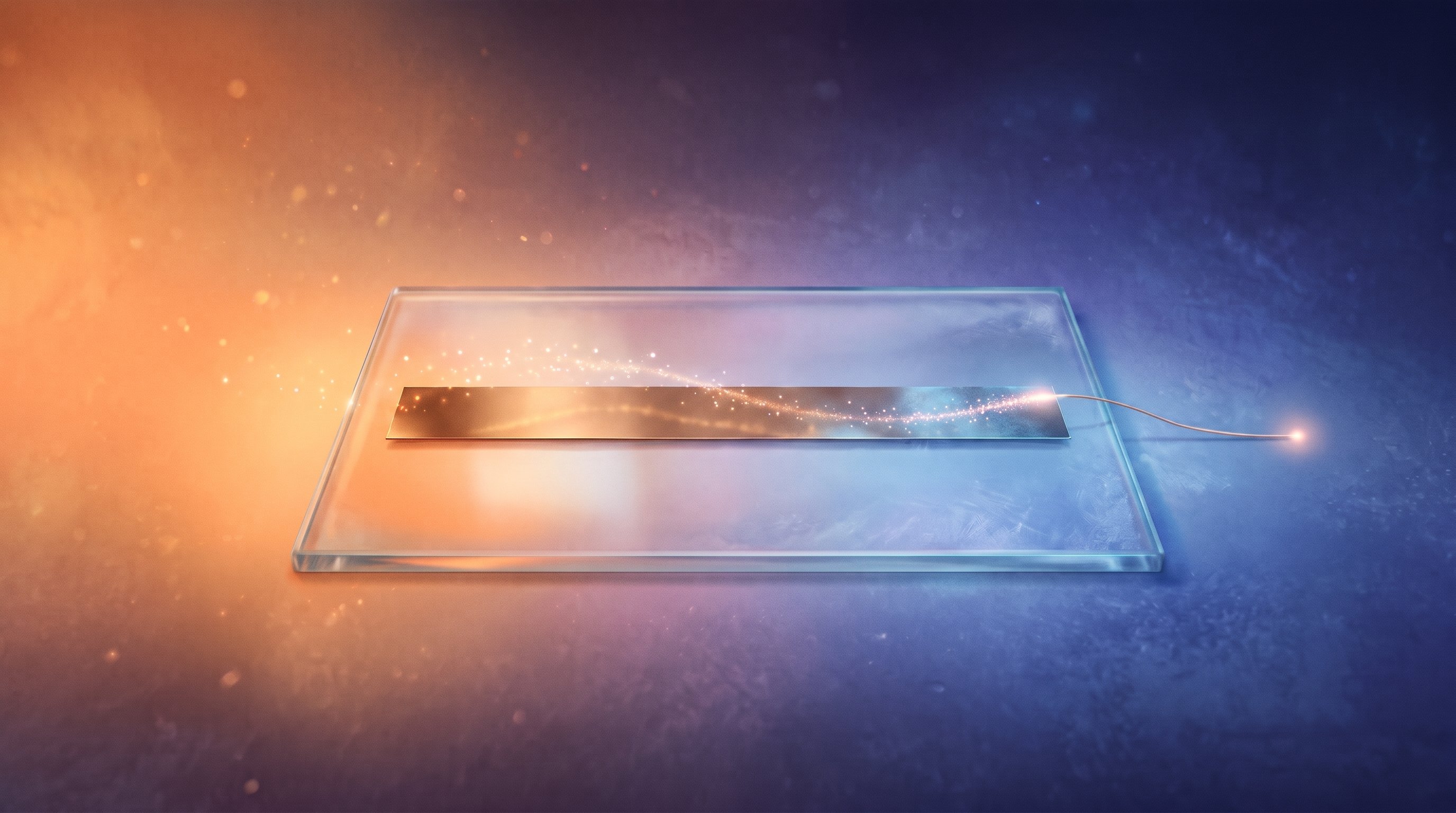
Researchers at Cornell University in the United States have made a semiconductor with a band gap of more than 7 electronvolts. According to the university, this is the widest ever in a working electronic device. With the material, aluminium gallium oxide with a little silicon in it, the team built a diode and a transistor, which they call AlphaFET. The research was published in October in the journal Nature; Cornell announced it on 3 November.
Why a wide band gap is difficult
In a semiconductor, an electron first has to cross an energy barrier before it can conduct current. That barrier is called the band gap. The higher the barrier, the stronger the electric fields the material can handle. This is useful for power electronics: the components that convert and control electricity, for example in an electric car, the power grid or the power supply of a data centre.
There is a drawback, though. The higher the barrier, the more the material behaves like an insulator: too few electrons get across the barrier, and the material hardly conducts at all. This is why the record for a working device stayed at about 6 electronvolts until now.
How they did it
Doctoral student Jacob Steele, from the group of materials scientist Darrell Schlom, grew the material layer by layer on a small plate of sapphire. At a low temperature, he added silicon. The silicon supplies the extra electrons that can carry current. Above 6 electronvolts, the layers conducted more than 100 million times better at room temperature than previously reported for such materials, according to the research.
Doctoral student Debaditya Bhattacharya turned the material into the diode and the transistor, under the supervision of professors Huili Grace Xing and Debdeep Jena. With the control electrode of the transistor, the team could make the current more than 10,000 times stronger or weaker. Xing describes them as first, preliminary transistors. Schlom says colleagues at first called the result impossible.
The next steps
With an electron microscope, researchers still saw many small flaws in the layers. Schlom compares this with other semiconductors in their early stage: once these flaws disappear, there is plenty of room for improvement. Jena says more work is needed to make the components suitable for practical use, and calls the material a promising platform.
One advantage is the sapphire. It is cheap and is already made on a large scale, unlike some other wide band gap materials, which are difficult and expensive to make in usable sizes. Jena names electric drives for vehicles and aircraft, power electronics for data centres and lasers for telecom among the possible uses.
What does this mean for the road to the singularity?
Power electronics are found everywhere that electricity is converted, including in the data centres where AI models run. Components that can handle higher voltages can make that infrastructure more efficient. This is a first step: a material that in theory looked too much like an insulator now works in a transistor. If the flaws in the layers disappear, more efficient electronics for the power grid, electric transport and computing power come a good deal closer.
What is the technological singularity? Read the explanation →