Nederlands
Lam Research and imec make ultra-fine ruthenium chip wiring in a single exposure
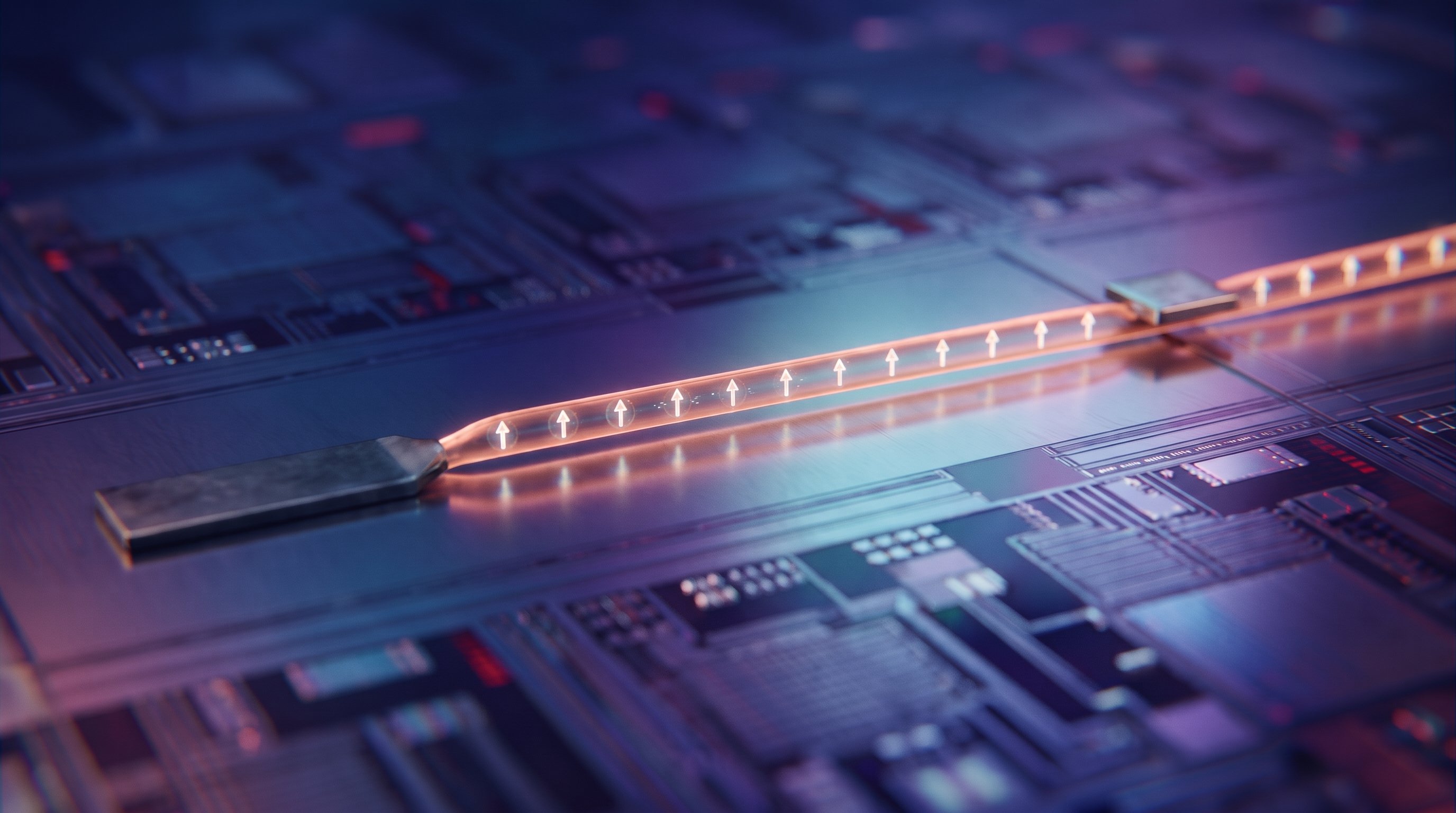
Lam Research and the Belgian research centre imec made metal chip wiring with lines that, together with the gap between them, are 20 nanometres wide, in a single exposure on ASML's newest machine. All short-circuit test structures worked. The next step is production.
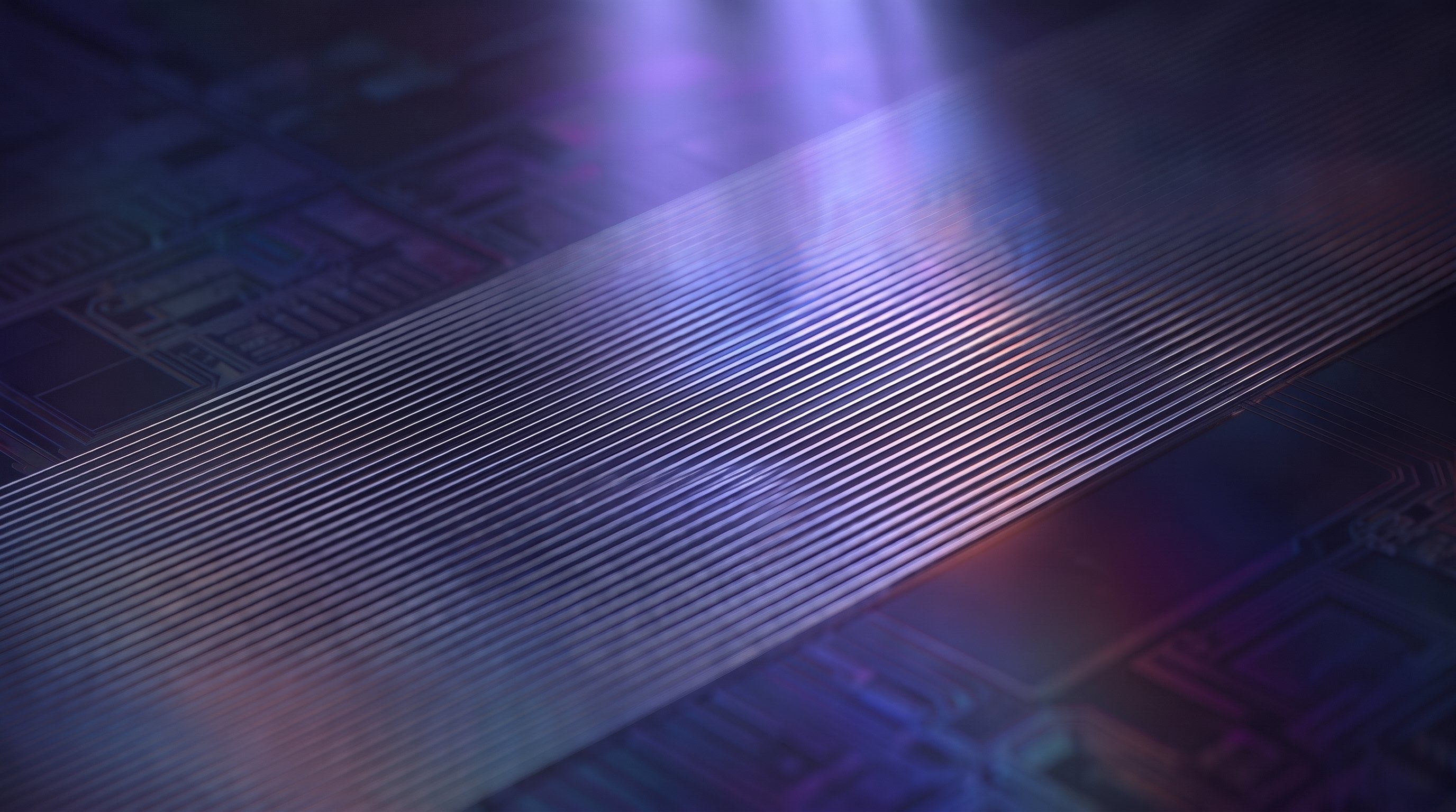
The American chip equipment maker Lam Research and the Belgian research centre imec have shown that they can make extremely fine wiring for chips in one single step. For this they used the metal ruthenium, a new kind of light-sensitive layer from Lam and a high-NA EUV machine from ASML: the newest and most precise machine for drawing patterns on chips. Lam and imec announced the result on 27 and 28 October, together with a broader collaboration.
The metal lines lie so close together that a line plus the gap next to it is 20 nanometres wide. A human hair is about 4,000 times as wide. According to Lam and imec, all the test structures that check for short circuits worked, spread across the whole silicon wafer. Of the test structures that check for broken lines, more than 90 per cent worked.
Why chip wiring is becoming a problem
A chip consists of billions of tiny switches, called transistors. They are connected to each other by layers of metal wires on top of the chip. For more than 25 years these wires have been made of copper. But the smaller chips become, the thinner these wires have to be, and copper struggles with that.
There are two reasons for this. In a very thin copper wire, the electrons keep bumping into the walls, so the current flows less easily. On top of that, copper needs a protective layer around it, otherwise the metal leaks away into the chip. In very thin wires that layer takes up a large part of the space, leaving little copper to carry the current.
Ruthenium has fewer of these problems. The electrons in this metal are less hindered by the walls, and no protective layer is needed. That is why chipmakers see ruthenium as a candidate to replace copper in the very smallest layers. Ruthenium is also processed in a different way here: the manufacturer first lays down a thin layer of metal and then etches away what is not needed. That leaves only the wires.
Drawing with light, without small errors
To decide where the wires go, a machine draws the pattern with light on a light-sensitive layer, a bit like an old-fashioned roll of film. ASML's high-NA EUV machines can draw finer lines than any machine before them.
At this tiny scale, random small errors easily appear in the light-sensitive layer: a little bridge between two lines, which causes a short circuit, or a line that breaks somewhere. Lam has therefore developed a light-sensitive layer, called Aether, that is not poured onto the wafer as a liquid but laid down as a vapour. Developing the pattern, which makes it visible, is also done with gas instead of liquid. According to Lam, this leads to fewer of those errors.
It also matters that it worked in a single exposure. With such fine patterns, manufacturers today often have to expose a layer several times to make it. Every extra round costs time and money, and increases the chance of errors.
Broader collaboration
Lam and imec will also work together on stacking chips on top of each other and on future memory chips, in which memory cells lie in many layers above one another. In March 2026 imec received ASML's newest high-NA EUV machine, the EXE:5200, in its cleanroom in Leuven. That machine is part of the European NanoIC pilot line for chips smaller than 2 nanometres and should be fully ready for use by the end of this year.
The results were achieved in a research setting. The next step is to show how well the technique works in a factory that makes millions of chips day and night. Lam and imec have not yet said when chipmakers will start using the technique.
What does this mean for the road to the singularity?
AI needs more and more computing power, and much of that comes from chips with ever smaller parts. But smaller transistors help little if the wires between them no longer carry the current well. This trial shows that two new techniques work together: ruthenium wiring and a light-sensitive layer laid down as a vapour, on ASML's newest machines and in a single exposure. That brings a next generation of chips closer: more energy-efficient, faster and with more computing power per square millimetre, exactly what the AI systems of the coming years need.
What is the technological singularity? Read the explanation →